网站地图 | English / 繁中 / 简中
   
  专业晶圆制造服务
 
专业晶圆制造服务
专业技术
专业技术总览
GaAs & GaN RF Technologies
InGaP HBT
High Linearity InGaP HBT
High Voltage and GSM InGaP HBT
VCO InGaP HBT
GaAs PHEMT
HFET
GaN HEMT
Integrated Passive Devices
THz Schottky Diode
InP HBT Technologies
GaN Power Electronics Technologies
Optoelectronics Technologies
晶圆制造服务
  首页 > 专业晶圆制造服务 > 专业技术 > GaAs & GaN RF Technologies > InGaP HBT > High Voltage and GSM InGaP HBT
 
High Voltage and GSM InGaP HBT


High Voltage and GSM InGaP HBT (P5 & P6) power processes have been developed specifically for power amplifiers requiring operation at 8-10 volt bias and/or ruggedness under high VSWR conditions. GSM PA has demonstrated superior RF performance and can withstand more than 25:1 VSWR at 5V bias. Linear PA at 9V Vcc and has been demonstrated by customers for Infrastructure Driver Amplifiers. Both Processes have been in mass production since 2001.
Download PDF

High-Ruggedness InGaP HBT
Surpasses GSM PA’s RF Performance and Ruggedness Requirements
GSM 4W Power Cell Evaluation Board
PA performance
 
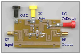
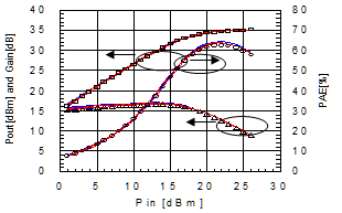
 PA performance* from 5 consecutive lots
 *Measured on the evaluation board (as shown)
  • Matched to 50Ώ
  • When matched for best power fficiency, PAE ~68%
  • Plotted data were not de-embedded
  • When de-embedded to device level, PAE ~74%
  • Device ruggedness: Survived >25:1 at 5V bias